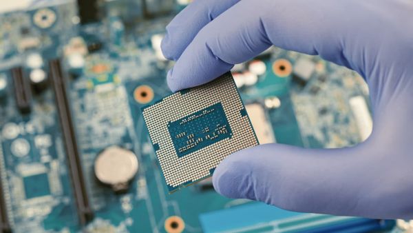
Johns Hopkins University researchers, together with international partners, have announced a discovery that could transform the future of electronics. They have developed a new class of materials and a novel process that makes it possible to build microchips smaller than ever before—so tiny they’re invisible to the naked eye.

For years, chipmakers have pushed the limits of microchip design to create devices that are faster, more powerful, and more affordable. But as chips shrink toward the nanoscale, traditional manufacturing methods have struggled to keep pace. High-powered lasers needed to etch ultra-small designs often don’t interact effectively with conventional materials, creating a roadblock for the industry.
The Johns Hopkins team tackled this by inventing a new approach called chemical liquid deposition (CLD). Using this process, they can apply ultra-thin coatings of specially designed metal-organic materials on silicon wafers with nanometer precision. These materials react strongly with advanced light beams, allowing manufacturers to carve out circuits at a scale smaller than today’s 10-nanometer standard.
Microchips are the “brains” behind modern electronics, powering everything from smartphones and cars to airplanes and household appliances. Making them smaller and faster while keeping costs low is critical for the next generation of technology—from artificial intelligence to space exploration.
“This process allows us to design materials that can keep up with the lasers and manufacturing systems already in place,” explained Michael Tsapatsis, a Bloomberg Distinguished Professor of Chemical and Biomolecular Engineering at Johns Hopkins. “It’s not just about going smaller—it’s about doing it efficiently enough to scale for the real world.”
The research, published in Nature Chemical Engineering, was a collaboration among Johns Hopkins University, East China University of Science and Technology, École Polytechnique Fédérale de Lausanne, Soochow University, Brookhaven National Laboratory, and Lawrence Berkeley National Laboratory.
By experimenting with different combinations of metals and organic compounds, the scientists discovered that materials like zinc could absorb “beyond extreme ultraviolet radiation” (B-EUV) more effectively than others. This makes them ideal for future chip designs, as B-EUV is expected to become the standard for microchip manufacturing within the next decade.
The breakthrough doesn’t just stop at one solution. The new framework opens the door to hundreds of potential material combinations, giving researchers flexibility to adapt to different manufacturing needs.
In Tsapatsis’s words: “What excites us is the range of possibilities. We now have a platform to customize materials for the chips of tomorrow.”
This development marks a significant leap forward in the global race to make microchips smaller, faster, and cheaper—an innovation that could reshape the electronics industry for years to come.