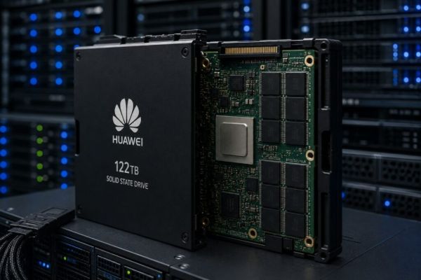
Huawei’s latest storage announcement may look like a routine product launch at first glance. A solid-state drive with capacities reaching 122 terabytes is large even by data centre standards, but capacity alone is not what has drawn attention across the semiconductor industry. What matters more is how Huawei appears to have built it.
For years, American export controls have focused heavily on limiting China’s access to advanced semiconductor manufacturing. Restrictions targeted leading-edge chips, semiconductor equipment and memory technologies tied to companies such as Micron, Samsung and SK Hynix. The assumption behind many of those controls was straightforward: if Chinese firms could not access the newest fabrication technology, they would struggle to compete in advanced computing and artificial intelligence infrastructure.
Huawei’s new SSD suggests the picture may be becoming more complicated.
According to technical details reported by storage industry publications, Huawei developed the drive using a packaging method that avoids dependence on high-layer-count 3D NAND chips restricted by American sanctions. Instead of relying on the latest Western memory technology, Huawei appears to have used proprietary die-on-board packaging methods that allow large numbers of NAND dies to be mounted directly onto the storage board itself.
The result is a drive reportedly capable of matching storage densities already used inside large artificial intelligence data centres elsewhere in the world. In practical terms, Huawei may have found a way to narrow part of the storage gap without waiting for Chinese semiconductor fabrication to fully catch up with overseas rivals.
The timing is important because artificial intelligence systems are placing enormous pressure on storage infrastructure. Large language models, recommendation engines and cloud computing systems process vast quantities of data. Companies building AI systems increasingly require storage measured not just in terabytes but in petabytes and exabytes. Capacity, energy use and data transfer speeds have become central concerns for cloud providers and enterprise computing firms alike.
That demand has pushed memory and storage makers into a new race. While graphics processors receive most public attention in AI discussions, storage systems remain just as necessary. AI servers cannot function efficiently without fast access to huge quantities of information. The larger the AI model, the larger the storage requirement surrounding it.
Huawei’s latest move shows how Chinese technology firms are adjusting under sanctions pressure. Since being placed on the American Entity List in 2019, Huawei has steadily lost access to many foreign technologies involving American intellectual property. That restriction affected everything from smartphone chips to cloud computing hardware and advanced memory products.
Yet sanctions also forced Chinese firms to rethink how systems are built. Instead of relying solely on access to the most advanced fabrication nodes, engineers increasingly focused on packaging, integration and system-level design. Huawei’s SSD appears to fit that pattern.
The technical idea behind Huawei’s storage drive is not entirely new. Traditional NAND flash memory packages usually place storage dies into compact units before attaching them to storage devices. Huawei’s approach reportedly removes parts of that packaging process and mounts the memory dies directly onto the printed circuit board using die-on-board methods.
That may sound like a small engineering adjustment, yet it changes the physical density that can be achieved using less advanced memory chips. Chinese memory supplier YMTC currently produces 232-layer NAND technology, which remains behind the newest memory products from Samsung and SK Hynix. Under normal circumstances, that gap would place Chinese storage firms at a disadvantage when building ultra-high-capacity enterprise drives.
Huawei appears to be addressing the problem through packaging density instead. By fitting more dies into the same physical footprint, the company can increase storage capacity even while using less advanced memory components.
This matters because export controls largely focused on fabrication chokepoints rather than every possible form of systems engineering. Policymakers concentrated on preventing access to the most advanced manufacturing tools and chips. Yet semiconductor progress does not always depend entirely on process nodes. Packaging, cooling, power management and software optimisation increasingly shape computing capability as much as transistor size alone.
The broader semiconductor industry already reflects that reality. Nvidia’s AI systems depend heavily on advanced packaging. High-bandwidth memory systems rely on stacking and interconnect methods as much as fabrication technology itself. Apple, AMD and Intel all rely heavily on packaging design to improve computing density and energy efficiency.
Huawei’s SSD suggests Chinese firms are now pursuing similar approaches more aggressively under sanctions pressure.
There are still unanswered questions surrounding the drive. Huawei has not publicly disclosed detailed performance figures such as input-output operations per second, sustained transfer rates or long-term endurance under enterprise workloads. Those details matter because storage systems are judged not only by capacity but by speed, reliability and thermal management.
Yield rates may prove equally important. Packing large numbers of NAND dies directly onto boards creates engineering challenges involving heat, signal integrity and manufacturing consistency. Producing prototypes differs greatly from producing millions of reliable enterprise drives at scale. Whether Huawei can manufacture these systems efficiently for hyperscale deployment remains uncertain.
Still, the announcement alone carries weight because it shows China’s technology industry continuing to adapt under pressure rather than freezing in place.
Artificial intelligence has changed the economics of computing infrastructure. Before the AI boom, cloud providers focused heavily on processing efficiency and cost reduction. AI training systems now demand huge quantities of processors, memory and storage operating together at scale.
That demand is creating new winners across the semiconductor supply chain. Graphics processor companies surged first, but memory makers and storage firms soon benefited as AI workloads consumed larger quantities of data. Enterprise SSDs with extremely large capacities have become more valuable because they reduce physical space requirements and simplify large-scale server deployments.
Huawei’s move also reflects China’s wider attempt to reduce dependence on foreign technology suppliers. Beijing has spent years encouraging domestic production in semiconductors, cloud computing and telecommunications equipment. Sanctions accelerated that process by forcing Chinese firms to replace foreign technology where possible.
Chinese cloud providers and AI companies increasingly have fewer choices available. Restrictions affecting Nvidia chips, AI accelerators and memory products have narrowed access to foreign hardware. Domestic suppliers such as Huawei therefore occupy a growing role inside China’s AI market.
The political effect may prove just as important as the technical achievement. Export controls were intended partly to slow China’s progress in advanced computing infrastructure. Huawei’s storage announcement suggests that engineering workarounds can sometimes narrow the effect of those restrictions even when fabrication gaps remain large.
That does not mean sanctions have failed entirely. China still trails foreign rivals in several advanced semiconductor categories, particularly high-end lithography equipment and top-tier logic chips. Yet the storage announcement highlights how difficult it becomes to restrict an entire technology ecosystem once companies begin redesigning systems around the restrictions themselves.